Tag archives: nanotechnology
The May 2017 issue of Physics World is now out
 By Matin Durrani
Einstein’s equations of general relativity might fit on a physicist’s coffee mug, but solving them is no mean feat. Now, however, the equations have been solved in a cosmological setting for the first time, as Tom Giblin, James Mertens and Glenn Starkman explain in the May 2017 issue of Physics World magazine, which is now live in the Physics World app for mobile and desktop
Elsewhere in the issue, you can enjoy an interview with John Holdren, who spent eight years as Barack Obama’s presidential science adviser. Find out too about the good and bad of nanoparticles and explore the potential that skyrmions – magnetic quasiparticles – could hold as a new form of memory storage.
Don’t miss either this month’s Lateral Thoughts, in which physicist Roger Todd describes how his invention of a system for automatically watering his house plants almost led to a commercial device.
Remember that if you are a member of the Institute of Physics, you can read Physics World magazine every month via our digital apps for iOS, Android and Web browsers.
View all posts by this author | View this author's profile
NanoCars race on gold, sketchers invade Fermilab, physics of Thor versus the Hulk
By Sarah Tesh
Science has taken motor racing to a whole new, extremely small level with the NanoCar Race. The competition on 28 April will see nanoscale molecular machines “speed” around a gold racetrack for 38 hours. As the tiny-molecule cars are not visible to the naked eye, the race will take place inside a scanning tunnelling microscope (STM) at the Center for the Development of Materials and Structural Studies (CEMES), part of the National Center for Scientific Research (CNRS) in France. The teams behind the NanoCars control their vehicles using electric pulses but are not allowed to push them mechanically. Details about the cars and their teams can be found on this website, where you will also be able to watch the race later this month. There is more about the competition in the above video.
View all posts by this author | View this author's profile
Nanometre-scale printing technique could put its stamp on the electronics industry
By Anna Demming
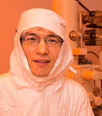
Qiangfei Xia in the lab.
This year marks 20 years since Stephen Chou, Peter Krauss and Preston Renstrom first published their work showcasing a versatile approach for mass production of identical nanostructures for the electronics industry. This technique is called nanoimprint lithography and it involves pressing a nano-patterned structure into a hot molten polymer. As the polymer cools, the pattern stamped into it sets so that it can be used as a mould to make several identical replicas of the original structure.
Just as the printing press brought literature to the masses, it is easy to imagine how this nanofabrication technique could have a significant impact on the production of integrated circuits. To commemorate the development, Nanotechnology has published a perspective article on the technique, and I had a chance to talk to the author Qiangfei Xia of the University of Massachusetts at Amherst about the technique’s advantages, challenges and outlook for the future.
Breaking the diffraction limit

The nanophotonics panel: Jennifer Dionne (left), Satoshi Kawata (middle) and Adarsh Sandhu.
By Hamish Johnston
At first glance, visible light and nanotechnology seem incompatible because of the diffraction limit, which dictates that features smaller than about half the wavelength of light cannot be resolved optically. For visible light, the diffraction limit is about 300 nm and this means that there is no point in trying to make conventional optical components that are any smaller.
But that pessimistic outlook has changed over the past decade or so thanks to the development of nanophotonics, which makes use of near-field (or evanescent) light and plasmons to manipulate light on length scales much smaller than the diffraction limit. Today, nanophotonics is being used across a range of disciplines, including biological imaging, telecommunications, solar energy and semiconductor processing.
View all posts by this author | View this author's profile
Physics World 2014 Focus on Nanotechnology is out now
By Matin Durrani
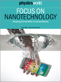
One of the beauties of physics, I’m sure you’ll agree, is that it stretches from the very big (cosmology) to the very small (particle physics). In fact, the great questions at the heart of those fields may well have attracted you to physics in the first place. But a lot goes on in-between these extremes, not least at the nanoscale. It might lack the glamour of research into dark energy or the Higgs boson, but nanotechnology has far more of an immediate impact on everyday life than physics at either end of the length scale.
If you want to find out about some of those applications, take a look at the latest Physics World focus issue on nanotechnology, out now in print and digital formats. It covers, for example, the work of the UK firm P2i, which has developed a “dunkable” nano-coating that can keep a mobile phone functioning after being submerged in water for up to half an hour. Could be handy next time you go swimming.
The Physics World 2013 Focus on Nanotechnology is now out
By Matin Durrani
There’s just one purpose to this blog entry – to get you to check out the latest Physics World focus issue on nanotechnology.
Created in collaboration with our sister website nanotechweb.org, the new focus issue, which you can read in digital-magazine format simply by clicking this link, is packed with great content including a feature by Nobel-prize winning physicist Kostya Novoselov, who shared the 2010 prize with Andre Geim for their work on graphene.
View all posts by this author | View this author's profile
Glass-blowing at the nanoscale
By James Dacey
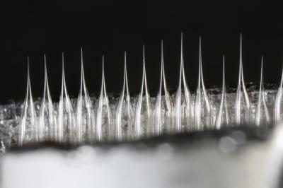
From the Romans to the studio artists of today, glass blowing is as much an art form as it is a technical discipline. In the same spirit as this creative lineage, a group of researchers in Switzerland has invented a technique for creating nano-sized capillary tubes of bespoke sizes.
View all posts by this author | View this author's profile
