By Margaret Harris
The Harwell Science and Innovation Campus added another jewel to its crown yesterday when the industrial-diamonds firm Element Six officially opened its £20m new R&D facility on the Oxfordshire site, which is already home to organizations such as the Rutherford Appleton Laboratory and the UK’s flagship synchrotron, the Diamond Light Source.
I’d heard about Element Six’s plans thanks to this article, which appeared in the careers section of June’s Physics World. The author, Stephanie Liggins, is a physicist who joined Element Six after completing her PhD at the University of Warwick, and towards the end of the article she mentioned that she would soon be moving to the company’s new Global Innovation Centre – which she described as “the world’s largest synthetic-diamond research and development facility”.
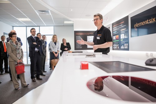
That sounded intriguing, so when I got an invitation to attend the centre’s gala opening on 3 July, I trotted off to Oxfordshire. Upon arrival I was ushered into a tent outside Element Six’s new building, along with dozens of industry leaders, government officials and people wearing scarves and ties in the company’s signature orange hue (“A bit like the Dutch football team – or EasyJet,” said one wag). After speeches by Element Six chairman Philippe Mellier and the UK science minister, David Willetts, we were allowed into the building along with a gaggle of orange-and-black-wearing tour guides.
The first stop on my tour was the chemical vapour deposition (CVD) facility, where layers of diamond are formed in microwave-oven-like reactors that heat a mixture of methane and other gases to temperatures of more than 3000 K. In the CVD technique, diamonds are formed when carbon atoms “condense” out of the hot plasma and settle onto a substrate, building the crystal atom-by-atom “like a wall made out of bricks and mortar”, according to Ian Friel, a research scientist at Element Six.
Some of the diamonds created via this process, Friel explained, are used to make windows and other optical components for heavy-duty CO2 lasers. These diamond windows are, of course, more expensive than those made of cheaper materials such as zinc selenide, but for some applications, the extraordinary properties of diamond mean that the extra cost is justified. For example, diamond is well known for being hard and strong, but it is also transparent at a wide range of wavelengths, chemically inert (making it ideal for working with acids or other highly reactive chemicals) and extraordinarily good at conducting heat. In fact, it is such a good heat conductor that if you hold a disc of industrial-grade diamond up to an ice cube, the heat of your hand alone will make the disc cut through the ice like a hot knife through butter. (Doing this was my favourite part of the tour.)
With just 110 employees (including 40 who have transferred to Oxfordshire from previous, smaller R&D facilities in South Africa, Ireland and elsewhere in the UK) the new centre isn’t going to make much of a dent in the UK unemployment figures. But Element Six is definitely hiring, and this was evident at the opening, where several of the orange-clad people I spoke to said they had been with the company for weeks or months, not years. One more senior employee told me that they’re looking to recruit people with good communication skills as well as a background in materials science or a related area. If an interviewee can explain clearly and logically how they would approach a problem, she said, it may not matter if they don’t get the exact “right” answer – although, of course, it’s better if they can do both.
And, I suppose, if they can look good in orange while they do it.

It is good to see that the Harwell centre is moving into new hi-tech R&D domains. In my days there, there were a few fenced-in accelerators with lot of rabbits scurrying around in the grass as ogling companions.
Im ready to answer .Ask me please ? (smile)
Trackback: Blog - physicsworld.com
Trackback: Leaping across the innovation divide – MyPhysNet